Overview

ANF’s focus on next-generation quantum materials has directly resulted in usage by key companies in Canada’s rapidly growing quantum computing industry. The facility also enables Canadian researchers to compete at the international level in fields such as quantum computing, quantum devices, and photonics, among other impactful research areas.

ANF’s success in attracting key industry users can be attributed to its cost-effective access to advanced tools—such as one of Canada’s only photonic wire bonders—and providing high-level professional expertise for operating them. This is complemented by a short turnaround time for rapid research and development processes and flexibility in tailoring to specific requirements.

Services are offered on a per-use fee basis, which includes equipment training and professional assistance from the facility’s technical staff, Facilities Director Pinder Dosanjh, and Scientific Director Jeff Young.

Industry clients use the ANF for the design, hybrid integration, and testing of chips for applications in quantum computing, quantum networking, biomedical sensing, automotive LiDAR, and data communications.

As part of UBC Blusson QMI, ANF business and government partners also have access to 25 multidisciplinary teams of physicists, chemists, and engineers with expertise in areas including, but not limited to:

  • Materials synthesis
  • Quantum sensing
  • Clean energy
  • Quantum algorithms
  • Quantum computation

Fabricating qubits for D-Wave Quantum

D-Wave Quantum is primarily known for its quantum annealing (QA) technology based on superconducting flux qubits. Fluxonium, a relatively modern member of the flux-like qubit family, has also become an attractive candidate qubit for D-Wave Quantum.

Given the growing interest in fluxonium and D-Wave Quantum’s deep experience in building flux-like qubit quantum technologies, the company has embarked upon a research program that harnesses the unique properties of fluxonium for all of D-Wave Quantum’s technology development.

D-Wave has been collaborating with the ANF to prototype gate model quantum computing (GMQC) architectures based on fluxonium qubits. D-Wave’s scientific and engineering personnel work closely with ANF staff to design, fabricate, and package circuits using the facility’s state-of-the-art electron beam lithography (EBL) equipment and world-class EBL expertise.

Manufacturing precision Cryo-EM grids for brain health tech

Cryo-EM imaging technology, combined with AI, is an emerging method that could transform drug discovery by providing atomic resolution insights into the native structures of proteins implicated in disease. With cryo-EM, drugs and vaccines can be designed to specifically target and map precisely the desired sites for drug interaction on protein surfaces. One factor that is key to the success of the technology is preparing suitable specimens for imaging using cryo-EM. There is currently a major worldwide gap in the supply of suitable specimen supports (called grids) and limited options for customized design and manufacture of these grids.

By partnering with the UBC ANF, researchers from Djavad Mowafaghian Centre for Brain Health are now beginning to address this gap, both by leveraging existing technology for grid manufacture and by engineering novel methods to manufacture new grid supports for cryo-EM. This partnership allows the researchers to develop an efficient manufacturing process for the development of customized grids that meet stringent quality control measures. It also enables them to be independent of supply chain problems while simultaneously driving a successful and innovative interdisciplinary collaboration.

Rapid prototyping for Sonus Microsystems

Sonus Microsystems has developed high-performance, customizable, and versatile transducers with novel applications in healthcare, non-destructive testing (NDT), wearables, and beyond.Sonus had to experiment with many design variables, including a variety of materials and unusual substrates found in the microfabrication industry. In a standard cleanroom, this kind of process discovery would take months of work to implement, mainly because typical UV exposure systems and metal deposition systems cannot handle substrates other than a full-sized standard silicon wafer. 

Thanks to the equipment at the ANF, especially its maskless ML150 lithography system, Sonus was able to rapidly find the best UV dose for the different photoresists to test. This capability at ANF enabled the company to combine the equivalent of 20 separate experiments into a single run, saving them both time and funds. This machine, combined with the metal deposition systems at the ANF, also allowed Sonus to fabricate their transducers with unusual shapes and sizes. The capabilities of the ANF have allowed Sonus to decrease the development times of their prototypes and improve the performance of their devices, going from months to weeks.  

Partners

Nanofabrication Accelerator Program

Expressions of interest are now open for the second round of UBC Blusson QMI’s Nanofabrication Accelerator Program in partnership with the National Research Council of Canada Industrial Research Assistance Program (NRC-IRAP), Innovation UBC, and the Creative Destruction Lab-Vancouver.

The program will provide eligible small or medium-sized businesses (SMEs) with specialized nanofabrication services, including but not limited to:

  • Maskless photolithography
  • 100kV electron-beam lithography
  • Photonic wire-bonding
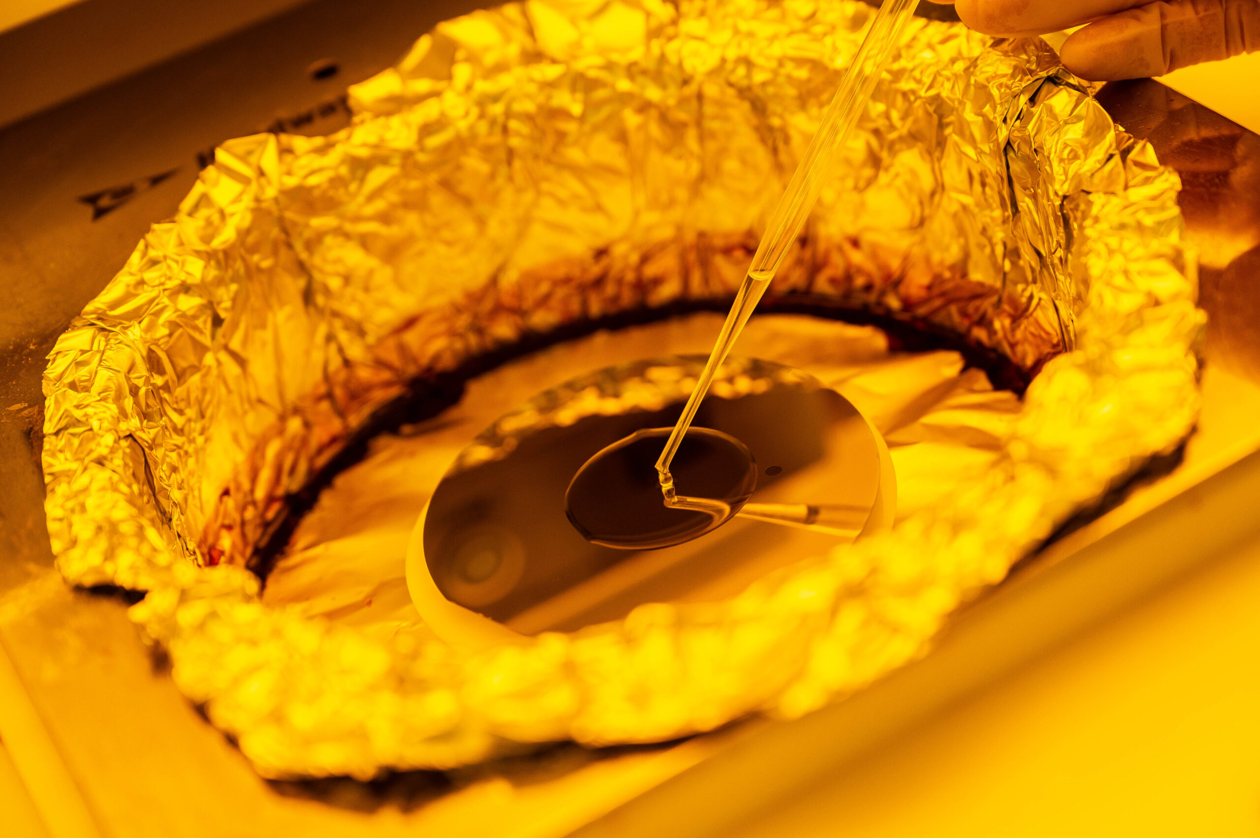
  • Thin film deposition and etching processes

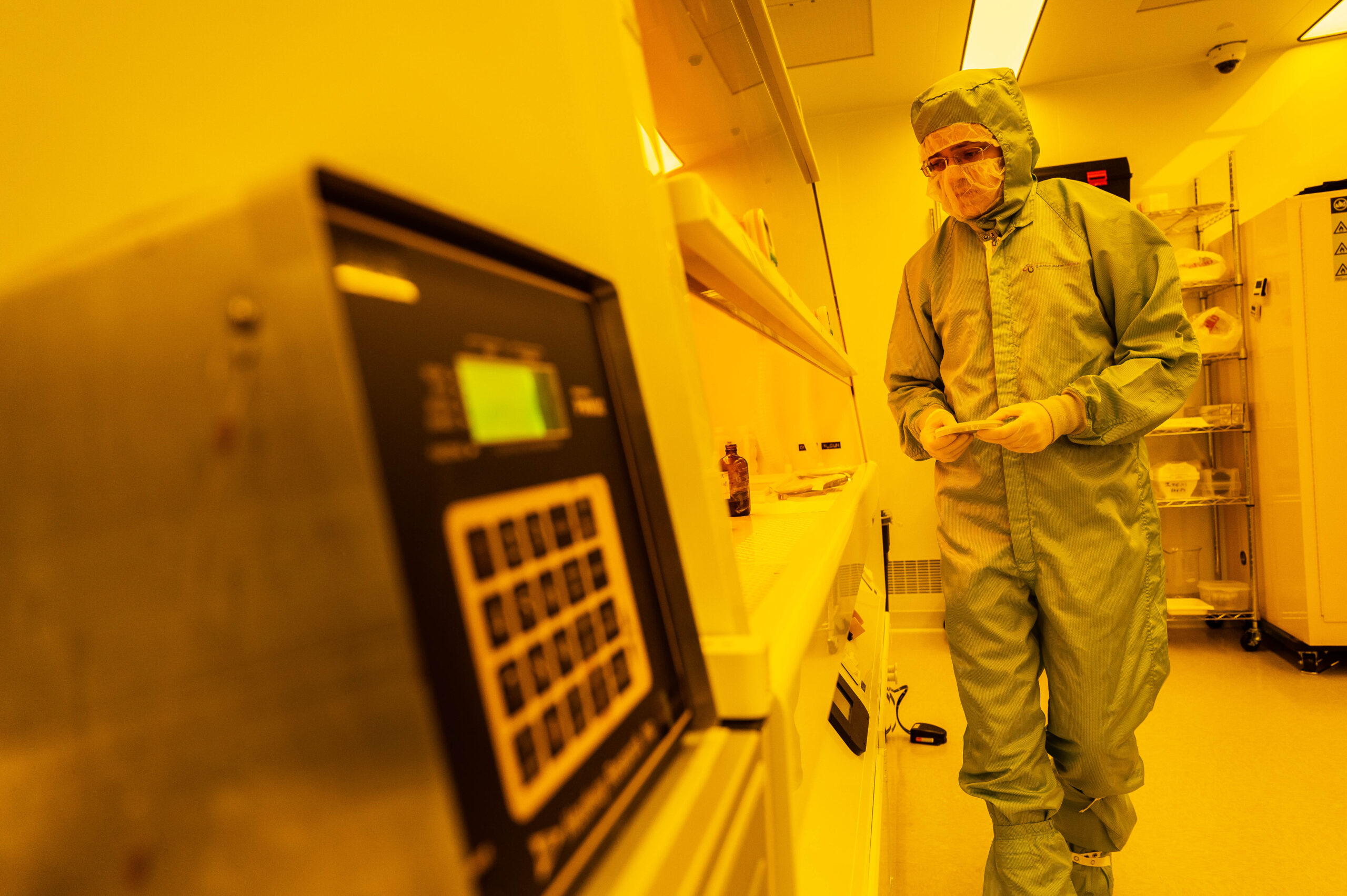
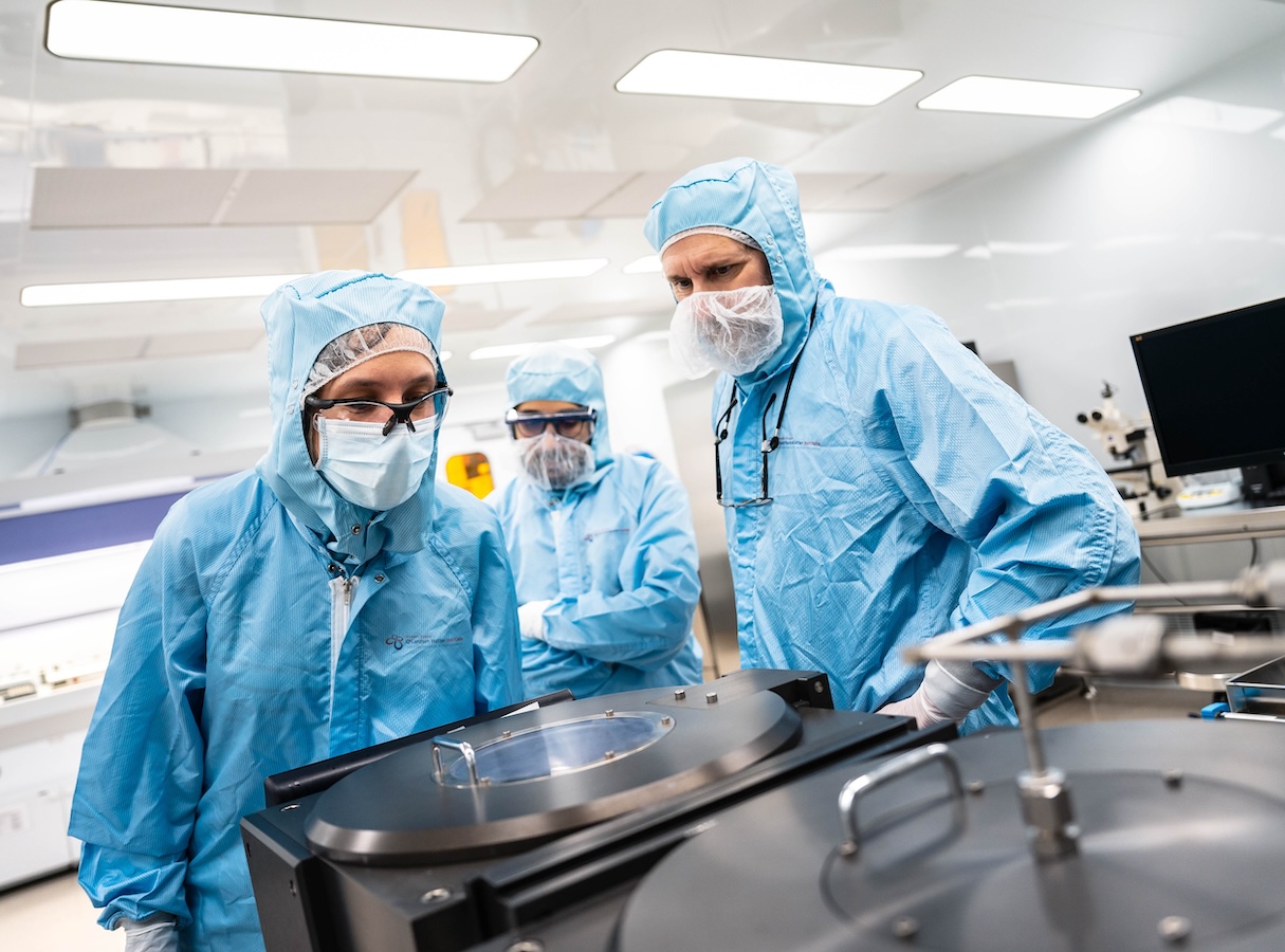
Companies will have access to recently upgraded cleanrooms. Services will be offered on a per-usage fee basis, including SME staff training for using the various tools and professional assistance from the facility’s technical staff. Up to $18,000 of funding is available per SME project, each of which will be limited to a maximum of 6 months in duration.

Expertise & Industry Applications

As part of UBC Blusson QMI, ANF partners have access to 25 multidisciplinary teams of physicists, chemists and engineers with expertise in areas including but not limited to materials synthesis, quantum sensing, clean energy, quantum algorithms, and quantum computation.

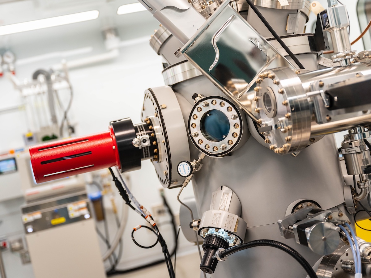
Current industry clients use the ANF for design, hybrid integration and testing of silicon photonic chips for applications in quantum computing, quantum networking, biomedical sensing, automotive LiDar and data communications.

Program Timeline

The program is scheduled to run until September 2025 and can accommodate only a limited number of projects.

How to Apply

SMEs interested in taking advantage of our enhanced technical innovation capabilities for enabling faster technology deployment and commercialization in their relevant industrial sectors are therefore being called to submit an expression of interest by contacting UBC Blusson QMI Facilities Director Pinder Dosanjh at pinder.dosanjh@ubc.ca.