Two breakthroughs in the 2000s dramatically broadened the field of 2D materials research. One was the development of methods to grow atomically perfect stacks of less common materials, leading to phenomena such as magnetism and superconductivity that are elusive in semiconductors.

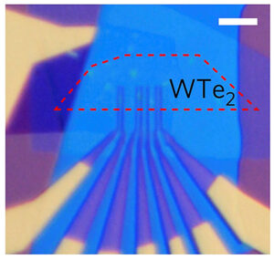
The second was the discovery of graphene, single atomic layers of graphite, resulting in an explosion of work on compounds that could be exfoliated like graphene and assembled into “van der Waals” stacks. Such 2D materials offer access for engineering via a third spatial dimension, either by stacking dissimilar materials or local gating. They are also amenable to study by powerful techniques for probing surfaces since they are mostly surface.

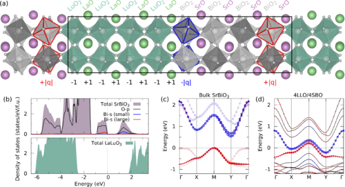
The field of 2D materials research proliferated rapidly thanks to those two discoveries, with the development of new stacking controls such as strain and twisting of layers, and recipes to grow more exotic materials combinations. The discovery of novel phases of matter in 2D has also been fueled by ideas from Blusson QMI theorists, including Marcel FranzIan AffleckGeorge Sawatzky, and Mona Berciu, in step with our fundamental principle of quantum materials-by-design.

The 2D Grand Challenge team will bring these new ideas to fruition with an array of new experimental capabilities under development within the Institute. Ke Zou’s team has established a lab for growing atomically precise heterostructures by molecular beam epitaxy (MBE), combining growth capability for two challenging families of materials (transition metal oxides and chalcogenides) with experimental chambers where measurements can take place. In parallel, Ziliang Ye’s and Josh Folk’s groups have built a facility for exfoliating and stacking 2D materials, equipped with cutting-edge techniques to keep the Institute at the forefront of the field.

Through this Grand Challenge, we will connect these different growth capabilities with the expanding range of experimental probes being developed by Sarah Burke, Doug Bonn, David Jones, and Andrea Damascelli.

The team is aiming at three target areas:

Flat band physics by design

Engineering Moire and strain to create correlated phases from conventional materials, where kinetic and Coulomb energies of the electron system are comparable. Building on Blusson QMI’s expertise in the physics of 2D materials including cuprates, we will investigate connections between these two systems: one tuned by chemistry, the other by twist angle.

Building topological superconductors

Van der Waals and MBE approach to creating 2D superconductors hosting Majorana excitations. We will grow a topological version of iron-based superconductors in monolayer form, aiming for a material that can serve as a basis for topological quantum computing. A parallel strategy, originating within Blusson QMI, is to induce topological order into a well-known superconductor by clever stacking.

Bose-Einstein condensates from electron-hole pairs

Starting from stacked chalcogenide or oxide interfaces, we aim for a new generation of devices that promise orders-of-magnitude higher transition temperature and unprecedented maneuverability compared to earlier realizations in cold atom systems.

Out of the novel phases of matter that emerge from these experiments, we aim to develop devices that influence future generations of quantum technologies and shed light on some of the deepest mysteries of quantum matter.

Rendering of monolayer tungsten ditellurite.

Figure 1: Exfoliated monolayer tungsten ditellurite sandwiched by hexagonal boron nitride.
Optical image (scale bar, 5 μm) of a monolayer WTe2 sample with two graphite gates, showing current, voltage contacts, and ground configuration for measuring the four-probe resistance Rxx. (Sajadi, Palomaki, Fei, Zhao, Bement, Olsen, Luescher, Xu, Folk, Cobden (2018)) Sample was fabricated by exfoliation and dry transfer method. Transport measurement shows monolayer tungsten ditelluride can be both a superconductor and topological superconductor controllable by gate voltage.

Research into the physics of 2D materials is central to this Grand Challenge.

Figure 2: The “quantum sandwich” heterostructure LaLuO3/SrBiO3
The black rectangle indicates a unit cell, which is periodically repeated along with three spatial directions and to be grown by MBE method. (Khazraie, Elfimov, Foyevtsova, Sawatzky (2020)) Within the polar LaLuO3 layer, the LuO2 monolayers with a nominal charge of -1 electron charge per Lu are alternating with the LaO monolayers with a charge of +1 electron charge per La, which results in the accumulation of electrostatic potential across the LaLuO3 layer. This triggers a transfer of charge -|q| from the large BiO6 octahedra at the SrO/LuO2 interface (highlighted in red) to the small BiO6 octahedra at the LaO/BiO2 interface (highlighted in blue).

Principal Investigators

Current Opportunities

Blusson QMI is looking to fill a number of important positions for this high-profile project. The team will work closely together to deliver the objectives set out above. Postdoctoral fellows will be expected to exhibit leadership and be able to work independently to deliver results. Contact Ziliang Ye if you would like to find out more about the roles.