Facilities
Our purpose-built research and development infrastructure includes design, fabrication, and testing shops as well as space for large-scale experiments. Our facilities support our interdisciplinary research teams and their academic and industry partners. To learn more about our current partnerships and business opportunities please contact Pinder Dosanjh, Facilities Director, at dosanjh@phas.ubc.ca.
The tools you need, developed in-house, by expert staff
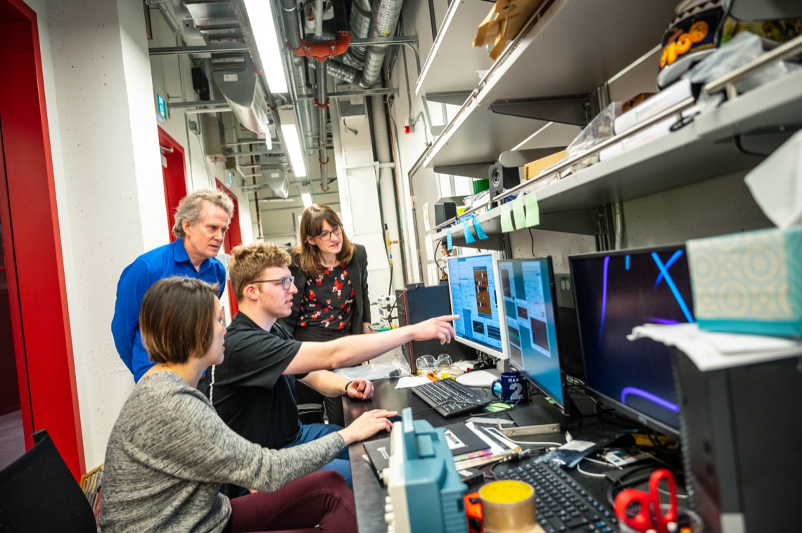
Our technical operations team and staff scientists, as well as machining and nanofabrication facilities, support our researchers, staff and students to develop the tools they need through designing, prototyping, and producing equipment, and by training and supervising users to create the parts and devices to customize existing research instruments in order to solve specific research problems.
Read: The tools for innovation from concept through creation
High Performance Computing (HPC)
The facility consists of 3 complementary clusters:
- LISA I (Laboratory for Interdisciplinary Science Applications, 1512 compute cores + 32 GPUs, optimized for parallel computation and density functional theory calculations);
- LISA II (128 compute cores, optimized for serial computation and tensor network calculations); and
- QuARC (Quantum Advanced Research Computing, 2176 compute cores + 8 GPUs, optimized for quantum algorithms operating on quantum simulators).
CONTACT
Pinder Dosanjh
Quantum Materials Design Laboratory (QMDL)
This is a facility for the discovery, crystal growth, and characterization of quantum materials in bulk form. This includes:
- more than 20 conventional furnaces for solid state, flux, and vapor transport growth;
- a high pressure multi-anvil apparatus for material synthesis under extreme pressures up to 10 GPa; and
- two floating zone image furnaces, including Canada’s only laser diode system, for the growth of pristine centimeter-scale single crystals.
QMDL also houses ultra-high resolution x-ray diffraction and four Quantum Design instruments for the complete characterization of the structural, magnetic, and electronic properties of quantum materials, at temperature between 0.05 and 1000 K and up to 14 T magnetic fields.
CONTACT
Alannah Hallas
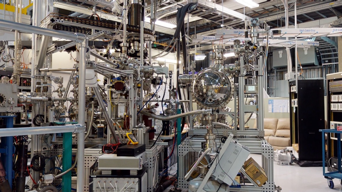
Quantum Materials & Devices Foundry (QMDF)
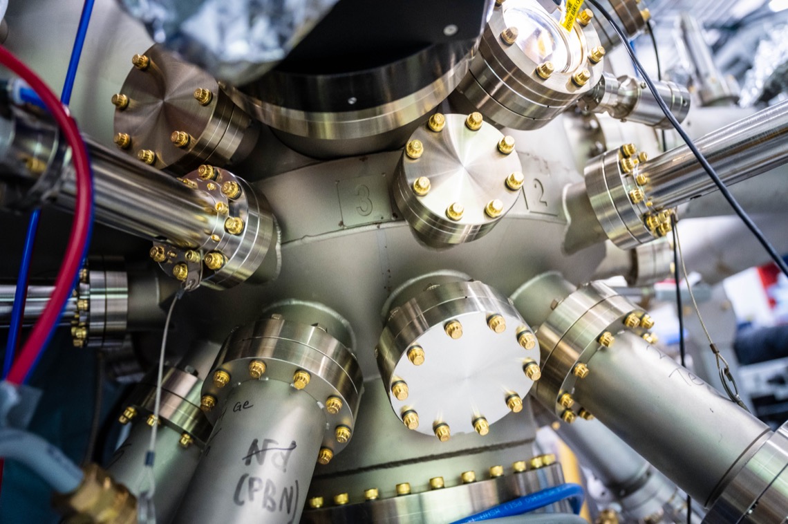
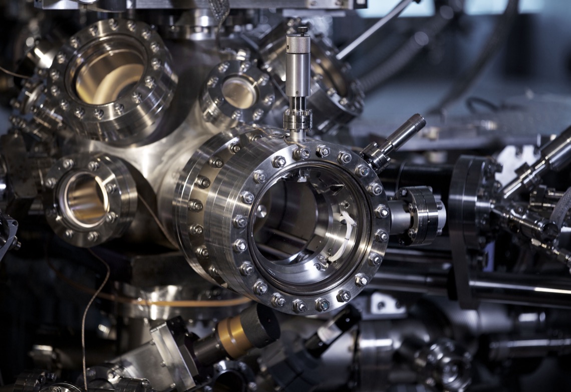
Integrates molecular beam epitaxy (MBE) synthesis of transition-metal oxides and chalcogenides thin films, layer-by-layer, with in situ angle-resolved photoemission spectroscopy (ARPES) and nanostructure fabrication techniques, to comprehensively characterize and engineer the electronic structure of quantum materials, and assemble them in novel heterostructures and gated field effect transistors (FETs). The twin-chamber MBE system has all the deposition sources and controls necessary to create a variety of superconducting, magnetic, and topological materials combining multiple elements, with fine control over the stoichiometry, and with the capability to fabricate heterostructures with excellent control of the surfaces and interfaces.
CONTACT
Ke Zou
2D Heterostructure Fabrication Facility
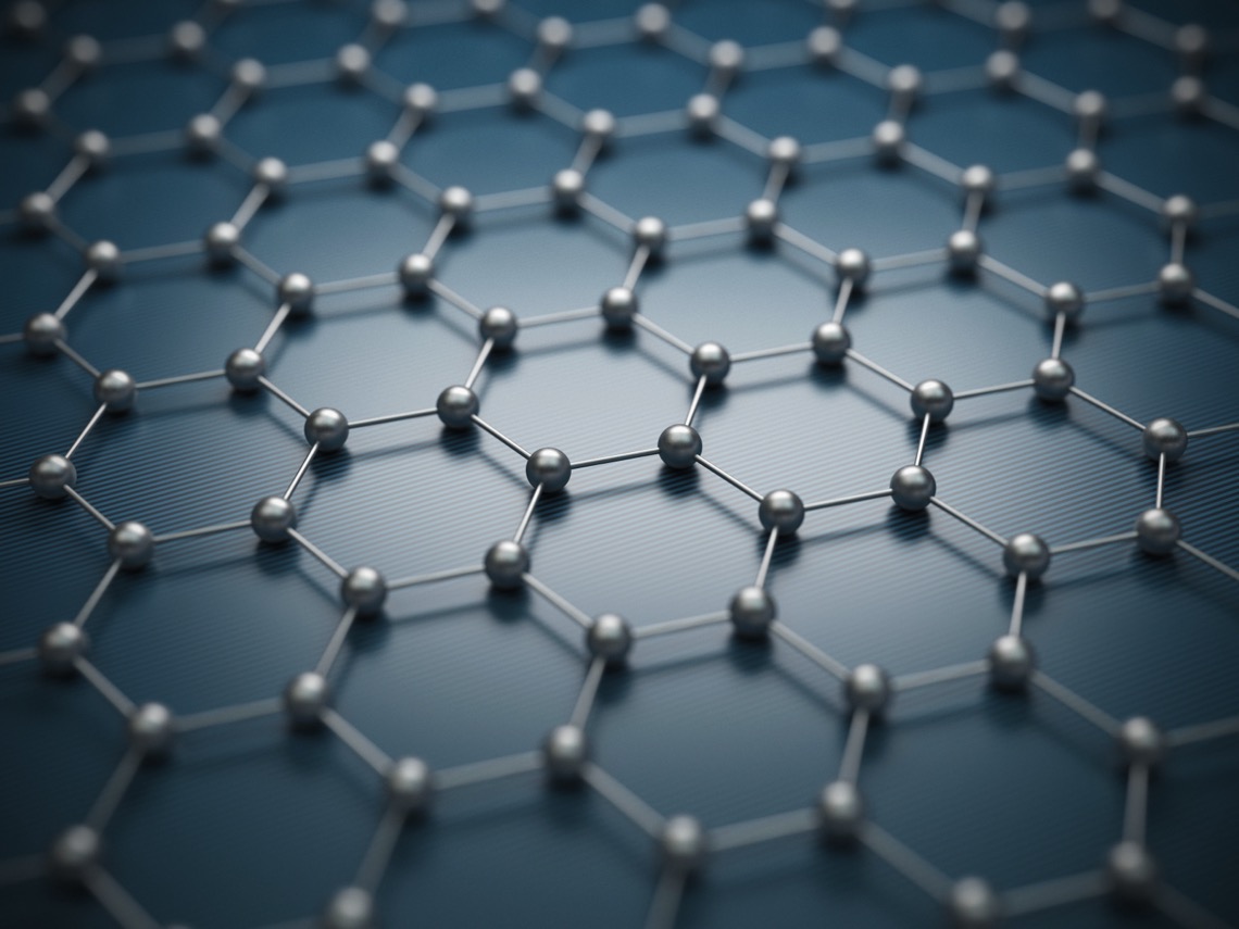
The facility allows the fabrication of atomically-thin twisted heterostructures and devices (aka twistronics) via the microexfoliation and stacking – with atomic precision at cryogenic temperatures and inert controlled atmosphere – of van der Waals (vdW) two-dimensional (2D) materials, such as graphene (superconductivity), transition metal dichalcogenides (photovoltaics and photodetectors), and high-temperature superconducting cuprates (single-photon detectors and topological qubits).
CONTACT
Pinder Dosanjh
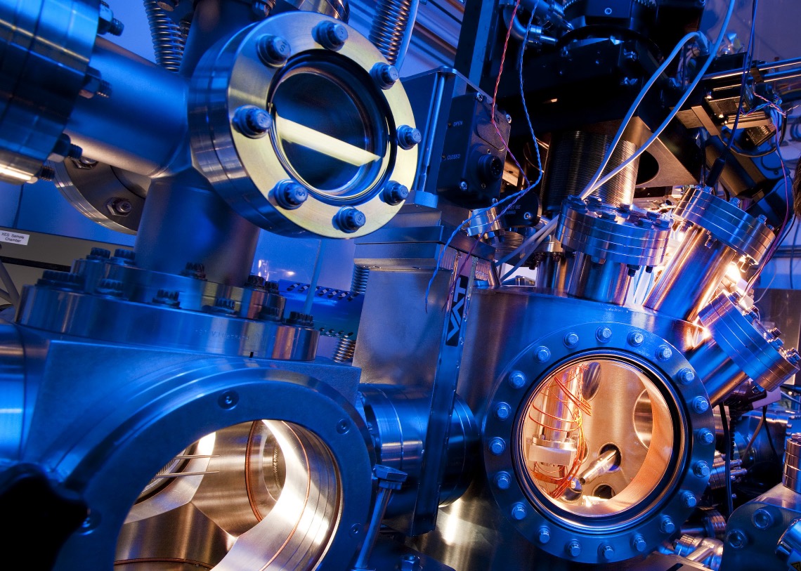
Quantum Materials Electron Microscopy Centre (QMEMC)
This unique-in-the-world facility is equipped with an aberration corrected NION transmission electron microscope (TEM) customed designed to combine atomic imaging with momentum-resolved electron energy loss spectroscopy (EELS). The system operates at cryogenic temperatures (liquid He), with unprecedented resolutions, and with the addition of external stimuli such as strain, and electric/optical fields. QMEMC is complemented by a nano-spectroscopy lab for optical and Raman spectroscopy measurements. These capabilities allow probing the momentum dependence of the dielectric function of quantum materials, collective excitations in inhomogeneous strongly correlated matter, and the spectrum of confined optical modes in new polaritonic materials based on 2D electrides and layered transition metal oxides, and developing means for exploiting them in quantum heterostructures and devices.
CONTACT
Pinder Dosanjh
Laboratory for Atomic Imaging Research (LAIR)
LAIR is a state-of-the-art facility for scanning probe microscopy and spectroscopy. It was specially developed to create independent extreme low-vibration environments for each of our five complementary, custom-designed instruments. With access to variable temperatures from milli Kelvin to room temperature, vector magnets up to 8 Tesla, 4 probe capabilities, and in situ material preparation, LAIR enables the study of electronic processes in quantum materials and devices at the nano and pico-scales, with impact in organic electronics, optoelectronics, and twistronics.
CONTACT
Pinder Dosanjh
UBC-Moore Centre for Ultrafast Quantum Matter
With its direct correspondence to the electronic structure, angle-resolved photoemission spectroscopy (ARPES) is a ubiquitous tool for the study of quantum materials, making it possible to map electronic band structures, Fermi surfaces, and interactions of electrons in a wide range of bulk and thin film single crystals. When extended to the temporal domain, by ultrafast pump-probe laser-based approaches, time-resolved ARPES (Time+ARPES) offers the potential to move beyond equilibrium properties, exploring both the unoccupied electronic structure and its dynamical response under ultrafast perturbation. The Moore Centre combines high-resolution ARPES with:
- a tunable pump and high-flux extreme-ultraviolet (XUV) tunable probe delivering 8-40 eV photons, to probe the out-of-equilibrium dynamics of electronic excitations with 190 fs temporal and 20 meV energy resolution;
- a tunable pump and a UV probe (6.2 eV) with tunable spatial resolution down to ∼11 μm, high energy (11 meV) and temporal (280 fs) resolution, for ground-breaking time-resolved μ-ARPES studies of 2D microexfoliated heterostructures such as ‘magic angle’ twisted bilayer graphene, mono and few-layer transition metal dichalcogenides, and high-Tc topological superconductivity in twisted bilayer cuprates.
CONTACT
Pinder Dosanjh
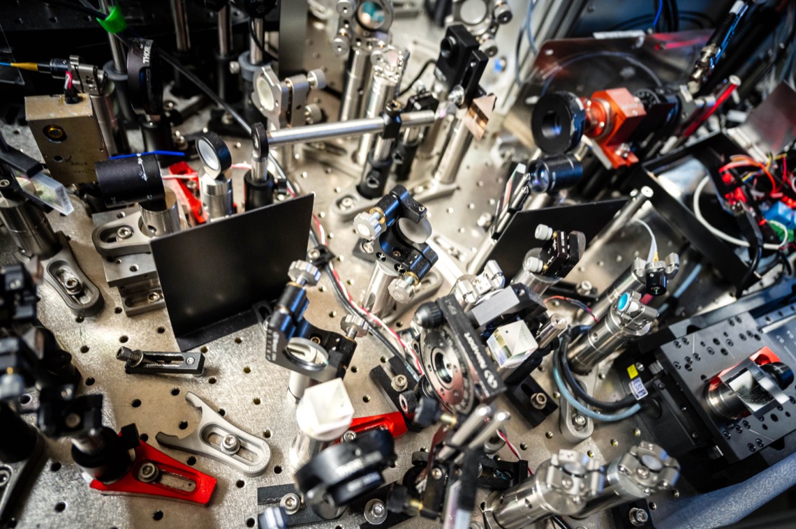
Ultrafast Optical Spectroscopy Laboratory
The laboratory encompasses the development of new and customized femtosecond laser sources and associated spectroscopic and imaging techniques, including continuous and ultrafast optical spectroscopy, scanning nearfield optical microscopy, ultrafast nonlinear optical spectroscopies, tabletop XUV ptychography, as well as advanced laser ablation spectroscopy, for the photonic manipulation of quantum states of matter, the nanofabrication of photonic devices, and the development of novel microscopy and quantum sensing techniques for applications in health, smart mining, renewable energy, advanced optical manufacturing, and quantum technologies.
CONTACT
Pinder Dosanjh
Quantum Materials Spectroscopy Centre (QMSC)
This bespoke beamline facility, developed and operated by Damascelli’s team and collaborators at the Canadian Light Source (CLS), integrates spin- and angle-resolved photoemission spectroscopy (Spin+ARPES) in two dedicated endstations to reveal the low-energy electronic and magnetic structure with high resolution, and to visualize the correlated motion of electrons in both bulk and thin film single crystals. The facility’s components — two elliptically polarizing undulators (15-1000 eV), beamline with two monochromators, two endstations, and integrated in situ MBE deposition chambers — are tailored coherently to form a premier international center for fundamental Spin+ARPES studies, and provide a complete snapshot of the electronic structure of a sample, and improve our control of the properties of quantum materials.
CONTACT
Pinder Dosanjh
Resonant Elastic/Inelastic X-ray Scattering (REIXS)
REIXS is a state-of-the-art beamline developed and operated at CLS by Sawatzky’s team and collaborators, featuring high flux, high coherence, and full polarization control, to visualize the electronic and magnetic structure of single crystals, thin films, and (buried) interfaces with high resolution and elemental sensitivity. It is suitable for studying novel quantum materials, including strongly correlated electron systems, spintronic materials, high-Tc superconductor, battery materials, and nano-scale biomaterials, and is unrivaled in unravelling complex behaviours such as spin, orbital, and charge ordering, and the ways that structural disorder, element distribution, chemical substitution, oxygen reduction, and ionic migration alters these behaviors.
CONTACT
Pinder Dosanjh
Quantum Science & Technology Lab (QSTL)
The laboratory develops and benchmarks qubits and nanoscale quantum devices (in extreme cryogenic environments), as well as quantum algorithms, to be exploited in quantum information technologies. QSTL is a state-of-the-art facilities to investigate:
- prototypes of future large-scale quantum computers involving superconductors and semiconducting materials of industrial relevance (QSTL is a world-leader in the nascent Ge spin-qubit technology); and
- quantum simulators, which are anticipated to be one of the first technological applications of quantum information and to enable laboratory tests of exotic aspects of many-body quantum theory.
QSTL’s quantum computing experimental effort in is tightly coupled to the development of quantum algorithms operating on quantum simulators enabled by the QuARC HPC cluster.
CONTACT
Pinder Dosanjh
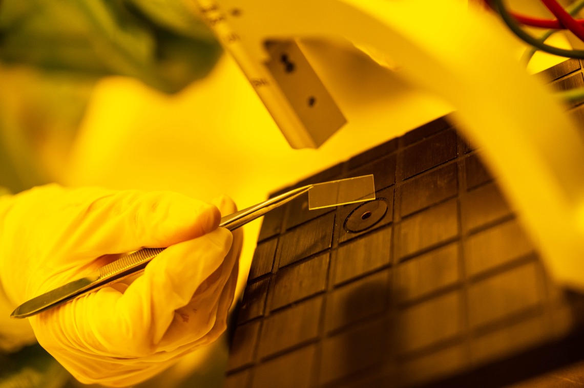
Advanced Nanofabrication Facility (ANF)
The ANF is the only nanofabrication cleanroom facility on UBC campus, and is the center for device fabrication for multidisciplinary applications including microfabrication of microfluidics devices (for proteomics, DNA sequencing, lab-on-chip, cell cultures), photonics (photonic crystals, lasers, modulators), nano-electronics (carbon nanotube devices, graphene electronics), and quantum devices (semiconducting and superconducting qubits). It plays a pivotal role in supporting academic users’ research (from QMI, UBC, and across Canada), as well as small and medium-sized enterprises (SMEs). While specifically designed for quantum device fabrication and processes in photonics, electronics, and quantum technologies, the ANF serves also major R&D efforts in clean energy, health, dentistry, and bioproducts.
Between 2016 and 2020, QMI and UBC (VPRI, Science, and Applied Science) invested significant resources (~$15M) in developing the ANF cleanroom space and associated equipment. With a floor area of 2,700 sq. ft., the ANF consists of two yellow rooms (ISO-5 and ISO-6) and one white room (Class ISO-6) on the top floor of the QMI budling, and an additional low-vibration white room (ISO-7) in the basement of QMI specifically designed for high precision lithography equipment. To support both academic and private sector fabrication efforts, the ANF is equipped with state-of-the-art instrumentation, including:
- hybrid and e-beam high-purity thin-film deposition systems, and furnaces for thermal treatments;
- optical and AFM microscopes, thin film thickness measurement systems, profilometers with 3D capabilities, and 4 point probes;
- contact (physical glass-mask) and maskless (software mask) photolithography systems, wet benches, photoresist spinners, and a wide array of dry and plasma ethers dedicated to specific materials (i.e., superconductors, metals, or semiconductors) or to the complete removal of photoresists;
- die and wire bonders;
- scanning electron microscopes (SEMs) and focused ion beam (FIB) system.
The jewels and centerpieces of the ANF infrastructure – heavily utilized by academic researchers and companies alike – are:
- the JEOL 100KeV Electron Beam Lithography (EBL) tool, located in the state-of-the-art vibration-isolation basement of QMI, used to write features as small as 5nm on quantum devices; and
- the Vanguard Photonic Wire Bonder (PWB), for integrating qubit designs with silicon photonics, opening up the possibility of upscaling quantum processors by implementing a single optical fiber communication rather than a multitude of microwave coaxial cables.
These two unique systems, combined with the ANF world-class cleanroom space and infrastructure, and QMI-CF’s world-class scientific and technical staff expertise, make the ANF the epicenter of the full quantum innovation cycle supported by QMI-CF.
MORE INFO